When I decided to make an alternative design for the bottom of the KBIC65 I eventually settled on trying my hand at creating a dithered image for my bottom PCB. This was a little trickier than I expected to get looking like I wanted but I really like the end result. When researching how to do it I had a hard time finding a good tutorial so I thought it might be worth sharing how I did it in the end, so you can produce something nice faster than me. The technique I use to scale and dither the image can be used for other types of engraving or printing, for example laser etching.
The general workflow is as follows
- Pick an image and crop away whitespace you do not want
- Resize the image to correspond to the manufacturing resolution
- Use a dithering tool to create a dithered binary version of the image
- Use KiCad bitmap2component to create a footprint from the dithered image
- Import footprint to your project
- Place it as mask or silkscreen
- Order PCB
- Enjoy!
At least in the best of worlds.
Pick an image
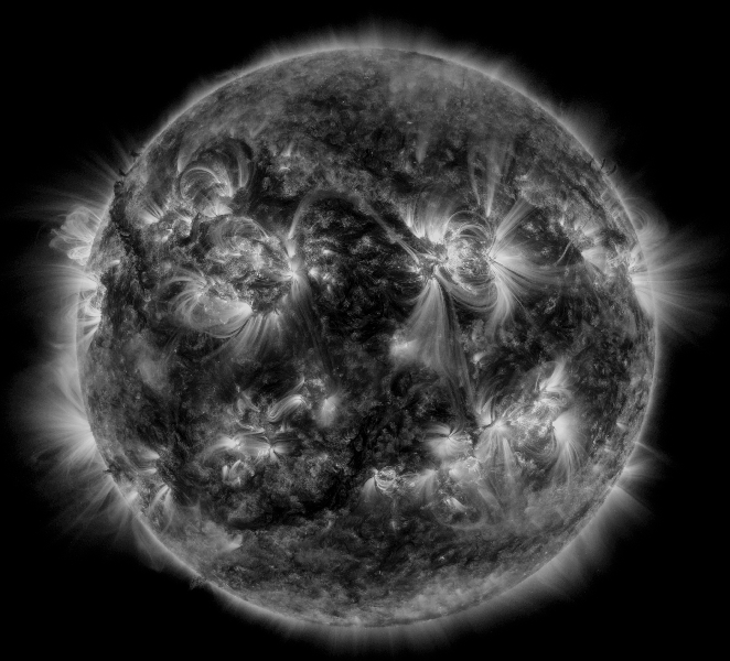
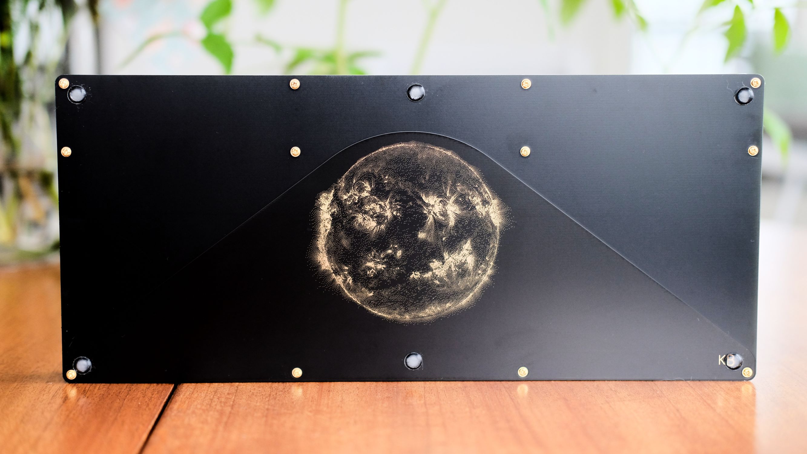
Settle on an image to use, crop it to only the part you want to place on the PCB. I settled on a NASA Solar Dynamics Observatory image.

Resize
JLCPCB and probably most other hobby-friendly PCB manufacturers can print at a resolution of about 0.15 mm, which is equivalent to about 169 DPI. JLCPCB actually a bit better, but 0.15 mm gives some margin. This means you should try to use 169 DPI or less and I used 169 DPI. Resize your image so that the resolution of the image at your selected DPI gives you the size you want on the board. I wanted my sun to be approximately 90 mm high so I resized to 600px high, which results in an image 90.2 mm high at 169 DPI.
Note If you want to create dithered art for some other tool, like a laser etcher, you simply just have to figure out the size of the smallest dot or line you can make, which is what I refer to as resolution, and calculate the corresponding DPI.
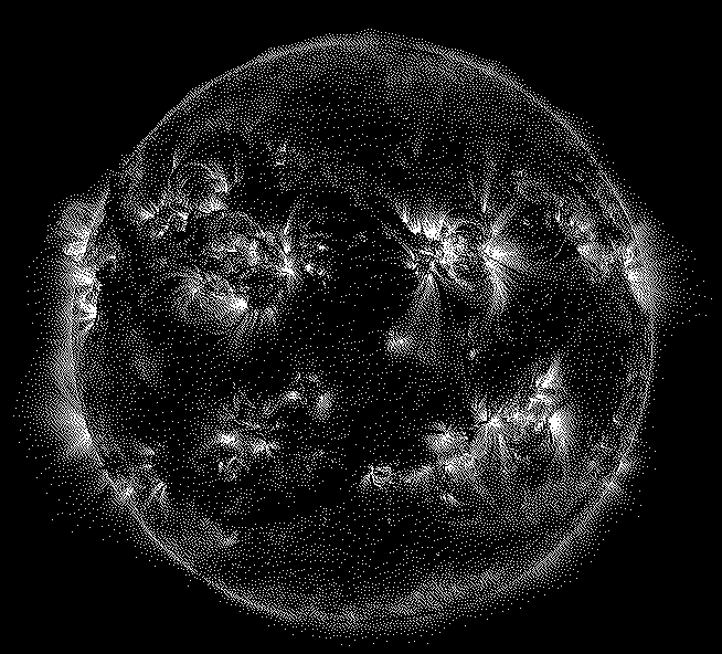
Dither
Use a dithering tool to dither your image and create a dithered copy. I strongly recommend Ditherlicious but you can look around for other tools you have handy. I also played around with dithering in Corel PaintShop Pro 2019, but didn’t like the result as much, and I believe Photoshop should have some tools for dithering. Once you have rendered your dithered image you should know that it might look funny, or not accurate, if you look at it using less screen pixels than the size of the image.
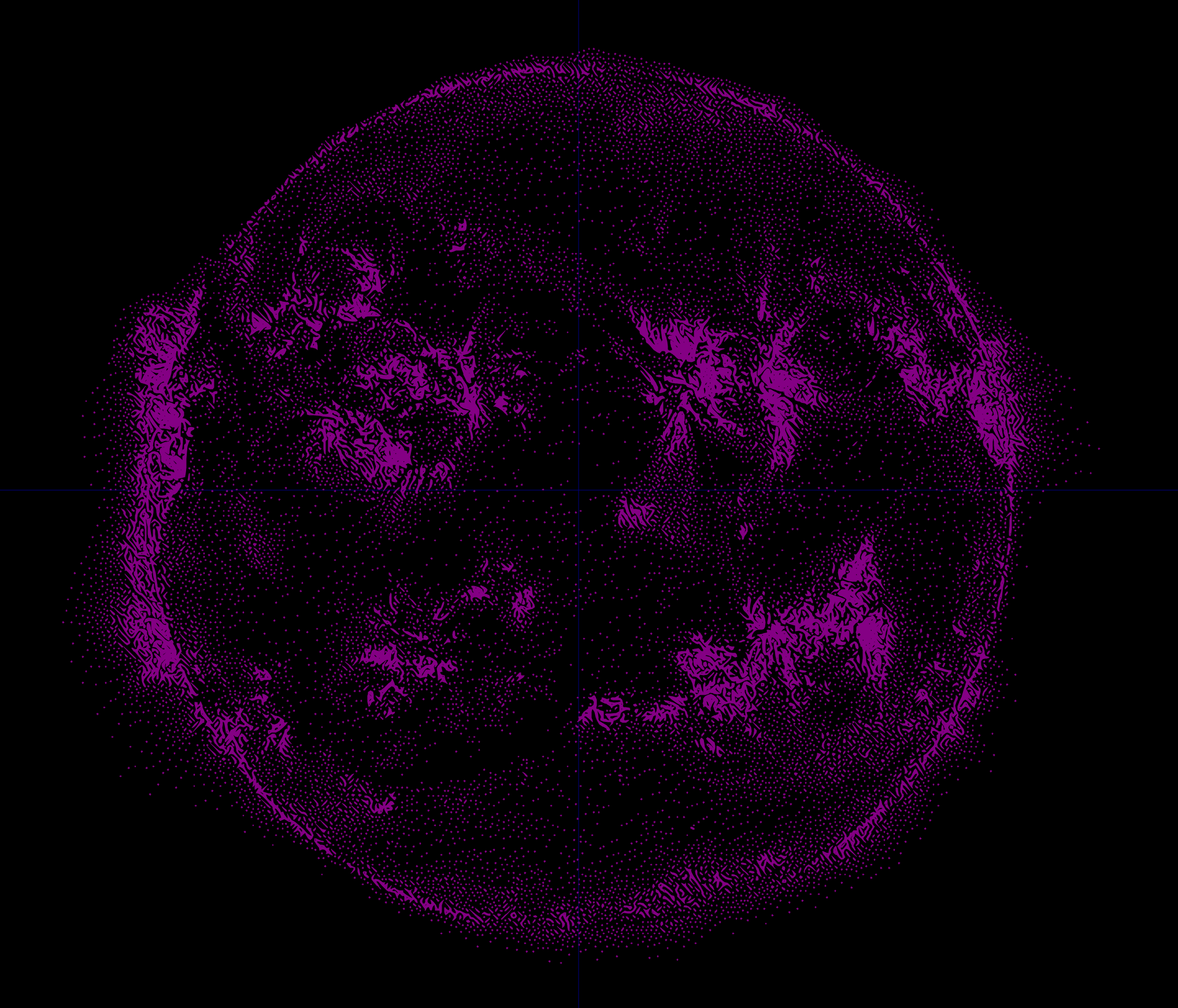
Create and import footprint in KiCad
- Open your KiCad project and then open Convert Image, a.k.a. the bitmap2component tool.
- Import your dithered image, select Negative if necessary, pick either Front Silk Screen or Front Solder Mask and enter your chosen DPI. Click export and put it into a new folder that will become a new KiCad footprint library for you.
- In Pcbnew or your KiCad project, open Preferences > Manage footprint libraries
- Add your new folder as a footprint library
- Import your new PCB art footprint onto your PCB
Iterate
Iterate, I played a lot with different dithering tools, changing the image contrast and exposure before conversion etc. The bitmap2component tool does not import dithered image exactly but blends pixels together, therefore I would recommend generating a few variants and comparing them in KiCad and possibly the 3D viewer. Personally, I think the resolution or separation of dots looks better in real life than what the footprint in KiCad did.
Warning Please note that these images requires quite a bit of processing from KiCad. Updating the 3D view especially, which took about 1-2 min for me on a semi-decent workstation.
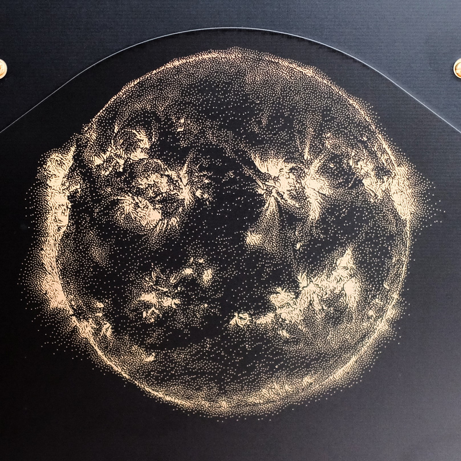
Manufacture
Final result after ordering from JLCPCB with black solder mask and ENIG finish.
And with a little more context on the back of the KBIC65.
Related links
- I found this project on Hackaday.io where the creator has tested printing different patterns to test the resolution. TL;DR if I was printing on silkscreen (instead of doing a copper mask) I would aim for 0.10 mm resolution.]
- You can also go crazy and do dithered full color PCB art.
- Some dithered PCB art experiments and discussion I used when figuring out my process
- Gerbolyze: Alternative tool I have not tried that adds a dithered image straight to the gerber files